Menu

News

Semiconductors

Tags

Chiral raises USD 12M seed

Chiral announced USD 12 million in seed financing led by Crane Venture Partners, with Quantonation, HCVC and Founderful participating, alongside public funding from Innosuisse. The ETH Zurich and Empa spin-off is developing equipment to integrate nanomaterials into semiconductor devices at wafer scale.

Its robotic system combines precision positioning, automation and process control to place materials such as carbon nanotubes onto silicon wafers. The funding will support improvements in throughput and reliability as Chiral installs its first commercial systems at customer sites.
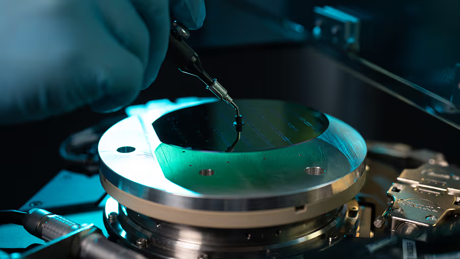
Semiconductor equipment. Image: Chiral

Tiny OLED pixels control the direction and polarisation of light

ETH Zurich researchers fabricated organic light-emitting diode pixels reaching the 100-nanometre size range using thin silicon-nitride stencil membranes. The method sharply reduces the feature sizes obtainable with conventional deposition masks. As a demonstration, the team made an ETH logo from 2,800 OLED pixels, each about 200 nanometres across, within a structure roughly the height of a human cell.

At these dimensions, closely spaced emitters can interact through optical wave effects. The researchers demonstrated control over emission direction and polarisation, extending the work beyond simple pixel miniaturisation. The Nature Photonics study points toward compact displays, sensing and electronically controlled optics. Individually addressing the nanoscale OLEDs remained an engineering objective, so the demonstration represents a fabrication and light-control platform rather than a finished high-resolution display.

Illustration of the nanoscale OLED ETH logo, with an enlarged detail and a cell-size comparison. Image: Amanda Paganini / ETH Zurich.

Stacked image sensors capture red, green and blue at each pixel

ETH Zurich and Empa researchers built two working thin-film image sensors that stack colour-sensitive perovskite layers vertically. By changing the material's chemical composition, each layer absorbs a selected part of the spectrum while passing other wavelengths onward. The arrangement lets each pixel measure red, green and blue without the side-by-side colour filters used in conventional silicon sensors.

The Nature study advanced the team's earlier single-pixel demonstrations into functioning sensor prototypes with different readout architectures. The approach promises better use of incoming light, more accurate colour reproduction and fewer demosaicing artefacts. Its theoretical threefold advantage in light collection and spatial resolution is a consequence of the stacked design. The prototypes still had pixels 0.5 to 1 millimetre across, leaving substantial lateral miniaturisation and readout development before consumer-camera applications.

One of the thin-film perovskite sensor prototypes. Image: Empa / ETH Zurich.

64-core analog chip runs neural networks using memory cells

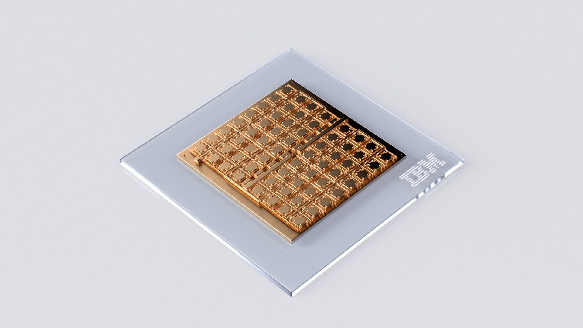
IBM researchers presented a 64-core mixed-signal chip that performs neural-network calculations using phase-change memory. Instead of repeatedly transferring stored weights to a separate arithmetic unit, the chip represents those weights through electrical conductance and carries out matrix operations within memory arrays. The design combines this analog computation with digital functions for processing activations and moving information between cores.

The international team included IBM Research Zurich's Manuel Le Gallo and colleagues working on in-memory computing. Manufactured in a 14-nanometre process, the research chip demonstrated inference on networks including image-recognition and recurrent models with accuracy approaching software implementations. Published in Nature Electronics, the work addressed how analog computing could support more complete neural-network workloads rather than isolated operations. The research processor brought analog memory arrays and their supporting digital circuitry together on one chip.

Illustration accompanying IBM's analog AI chip research. Image: IBM Research.

Scrona secures USD 6.7M Series A and USD 2.9M grant

Zurich-based Scrona announced USD 6.7 million in Series A investment and a separate USD 2.9 million grant from Switzerland's State Secretariat for Education, Research and Innovation. AM Ventures led the investment round, joined by TRUMPF Venture, Verve Ventures and Manz GmbH Management Consulting and Investment. Together, the two sources provided USD 9.6 million to industrialize and commercialize its printing technology.

The ETH Zurich spin-off develops electrostatic printheads that pull tiny droplets from a nozzle using an electric field. Its multi-nozzle approach aims to combine submicrometer printing precision with parallel production, including materials too viscous for conventional inkjet systems. Scrona planned to develop applications in semiconductor manufacturing, displays, electronics and printed circuit boards, including finely patterned layers for micro-LED displays.

Illustration of electrostatic material ejection in Scrona's printing process. Credit: Scrona, via Fabbaloo.

Confirm