Menu

News

Electronics

Tags

Winduction demonstrates bus charging through tyres

Winduction demonstrated an electric bus charging from a ground plate through coils in its tyres. Moving the receiving coils into the wheel reduces the transmission gap compared with underbody charging. The system needs specially developed steel-free tyres because conventional steel belts would absorb energy from the magnetic field as heat.

The company is building a laboratory and test bus stop in Winterthur before integrating the components for operation outside its private test area. Passenger trials are planned for 2028, with Swiss transport operators still in discussions. Smaller batteries and lower route costs are intended benefits, not results from a completed passenger-service trial.

Wheel-based charging concept; the video includes animation. Video: ETH News for IndustryWatch video

Open chip library cuts area and estimated energy use in design benchmarks

ETH Zurich researchers published benchmarks for EZ130 8T, an open library of 220 reusable circuit cells for IHP's 130nm chip-manufacturing process. In a post-layout matrix-multiplier comparison, the design used 35% less cell area and an estimated 39% less energy than the reference library, with a roughly 3% longer clock period.

Developed by students in a 2025 VLSI course, the library is available under Apache 2.0 and lets designers build chips from transistor-level components through automated design tools. Two chips using earlier versions passed initial tests, but full characterization is still underway. The reported efficiency gains come from design analysis, not measured silicon performance; the September preprint documents the results rather than marking the library's creation.

AND-gate layout from the EZ130 8T library, Figure 3a. Image: Oscar Castañeda and coauthors / ETH Zurich

OLED pixels can be patterned using chipmaking techniques

ETH Zurich researchers developed light-emitting polymers that also act as photoresists, allowing OLED materials to be patterned with chipmaking techniques. Reactive groups on the outside of each molecule cross-link under UV light, while a protective shell shields its light-emitting core from processing chemicals.

The team produced a 300 by 430 micrometre fluorescent test image and, separately, an electrically powered ETH logo measuring 1 by 2.4 millimetres. The fluorescent image is not a display, and a working screen still requires electronics to control individual pixels independently.

Microscopic fluorescent test image, 300 by 430 micrometres; not an electrically driven display. Image: Lo SW et al., Nature 2026 / ETH Zurich

ETHEREAL vision chip runs event-camera inference in 25.6 microseconds

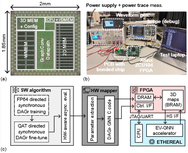
Researchers including UZH's Robotics and Perception Group demonstrated ETHEREAL, a processor designed for graph neural networks that analyse event-camera signals. Measurements on the DAGr-GNN workload and the 640-by-480-pixel DSEC dataset showed 25.6 microseconds of latency and 1.6 microjoules of energy per event-wise inference.

The chip combines parallel processing of neighbouring events with a memory design that caches relevant spatial and temporal information. It addresses the irregular memory access that makes these networks difficult to accelerate. The result is a measured research-chip demonstration, not a commercially available vision system; the August manuscript was submitted for possible journal publication.

ETHEREAL research illustration. Image: ETHEREAL authors / UZH Robotics and Perception Group.

Tiny OLED pixels control the direction and polarisation of light

ETH Zurich researchers fabricated organic light-emitting diode pixels reaching the 100-nanometre size range using thin silicon-nitride stencil membranes. The method sharply reduces the feature sizes obtainable with conventional deposition masks. As a demonstration, the team made an ETH logo from 2,800 OLED pixels, each about 200 nanometres across, within a structure roughly the height of a human cell.

At these dimensions, closely spaced emitters can interact through optical wave effects. The researchers demonstrated control over emission direction and polarisation, extending the work beyond simple pixel miniaturisation. The Nature Photonics study points toward compact displays, sensing and electronically controlled optics. Individually addressing the nanoscale OLEDs remained an engineering objective, so the demonstration represents a fabrication and light-control platform rather than a finished high-resolution display.

Illustration of the nanoscale OLED ETH logo, with an enlarged detail and a cell-size comparison. Image: Amanda Paganini / ETH Zurich.

Bota Systems raises USD 2.5M seed

Zurich-based Bota Systems completed a USD 2.5 million seed round led by Marathon Venture Capital, with participation from angel investors. The funding would expand the team and accelerate development of its force-and-torque sensing platform as the company served research laboratories and manufacturing customers internationally.

Bota's sensors combined sensing hardware, built-in electronics and software to give robots feedback about physical contact. This allowed robotic arms to adapt tasks such as polishing, assembly and handling, rather than depending only on precisely predefined movements. The company also described applications in automated electric-vehicle charging and hand-guided robot teaching. At the announcement, it reported customers in more than 30 countries and a network of distributors and robotics integrators across Europe, the Americas and Asia-Pacific.

Force-sensing hardware fitted to a robotic gripper. Image: Bota Systems.

Confirm